
![[Italian]](images/uk.gif)


PCMCIA Network Interface
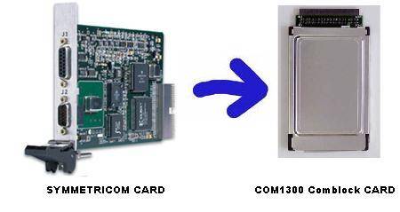
Main issue of the work presented in this section is to implement an FPGA-based PCMCIA card prototype capable of emulating Symmetricom�s bc635/637PCI card behaviour. This card acts like a receiver module that provides precision time and frequency reference to the host computer system via PCI bus and furnishes it to the TDP network processor for packets processing and queuing. Time is acquired from either the GPS satellites using a supplied antenna/receiver or from time code signals.
The card chosen for this purpose is the COM-1300 ComBlock module. It is a PC card which supports communication with a host computer either through a standard1 6-bit PCMCIA or 32-bit CardBus Type II bus interface. It is essentially composed by a Xilinx Spartan-3XC3S400-4 FPGA, internally connected to a 32 MB volatile SDRAM, a flash memory and a microprocessor and interfaced to extern world with the bus interface itself and a 40 pin connector. The whole system is provided with a 40 MHz clock internally generated by a quartz oscillator, but that may be replaced any time with an external source trough the assigned connector�s pin.
|
| New and Old card |
Software running within the FPGA basically follows the 4 points previously mentioned. By giving it a stable 10 Mhz squared wave input signal and a 1PPS one, it has to generate an interrupt signal that gives network server a precise time reference for processing packets that must be sent over the net. Interrupt signal has to be handled with the higher system priority in order to have faster response and reduce latency and for this reason, a dedicated driver has to be written. FPGA communication is memory mapped so, driver simply reads from and writes to registers, i.e acknowledging an interrupt, asking for current GPS time stamp or setting a new output frequency values.
"Plug and Play" PCMCIA bus solution ensures to this new prototype card to be compact, light and used with either laptop Pc or desktop. Higher portability and flexibility of the whole system that can be changed, carried and moved in a simpler way is one of the main task.
1 - FPGA Inplementation
Software running within the FPGA basically must satisfy 4 requirements:
- To accept a 1PPs signal sopurce input externally gathered.
- To generate an outupt frequency that must be programmabel by user and must be syncronized to the 1PPS signal.
- To communicate with a PC via PCI bus (or via PCMCIA-PCI bus) using interrupts signals to provide precise timing witht high priority and low delay to the network server
- To know the exact current time to recognise the correct packet posititon (position in Time Frame and Time Cicle domain).
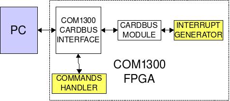
By givingit a stable 10 Mhz squared wave input signal and a 1PPS one, it has to generate an interrupt signalthat gives network server a precise time reference for processing packets that must be sent over thenet. This has been practically done by creating two separated VHDL processes within the FPGA:
- Interrupt generator concerns with the creation and handle of interrupts .
- Commands handler manages communication between PC and the card.
|
| Block diagram of FPGA-PCMICA |
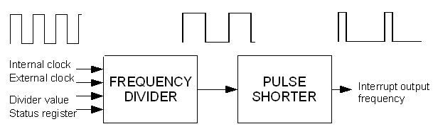
Interrupt signal is generated by a particular VHDL block that basically acts like a frequency divider. It takes the very stable 10 MHz input signals and lowers the frequency value according to the timing that is needed by network server to operate packet processing. Division is performed using a programmable counter driven by this 10 Mhz signal that changes output status signal any time count reaches the programmed value. This slowed-down version of the input squared wave signal is than processed to produce another signal that physically drives the interrupt line with the same frequency characteristic but a shorter pulse duration (i.e. max 100 us). This is needed in order to avoid interrupt line to be asserted for a longer time in case interrupt is not recognized by the system and so, not acknowledged.
|
| Input signal generation and processing |
Data exchange process between PC and card has been implemented as a FSM (Finite State Machine) that performs operations on data and commands sent by PC through the CardBus bus as shown in figure .
FSM is basically composed by 2 logical states:
- Idle state: here machine is waiting for a command from PC. Command flag (bit 2) of status register is continously checked and anything is done until it goes to high logical level. Than command is read from command register, decoded, executed and MSF prepares to go to next status.
- End state: Here nothing expecial is done but setting back the command flag to low level. This implies that PC is informed that command has been executed and card is ready for another operation. Than machine goes back to Idle status.
Communication is achieved by passing 32 bit command words to the FPGA input port that are than interpreted according to what previously presented in section \ref{Implement}. Since it is necessary to synchronize data exchange between PC and card and to buffer incoming or out coming data, an internal register structure is required. Registers are all 16 bit wide and used for:
- Status Register is the one that synchronizes data flowing and controls status of interrupt source and acknowledging. Any operation that is performed causes changes in this register flags according to what has to be done.
- Command Register is the register where a command is stored waiting to be performed. Every command that is sent to Comblock card needs to be acknowledged, in other words, any operation it is asked to do, must be followed by a particular command that informs card that a command has been sent to it. Bit 2 of the status register is used for this purpose; it is set to 1 by PC when a command is sent and then lowered by FPGA as soon as operation has been executed. This allows FPGA to take the time it needs to do a task before executing another one.
- Mask Register is used to control interrupt acknowledgement. This register is kept controlled by the com1330 driver's interrupt service routine. Since bit 1 of this register is set to 1 any time interrupt line is asserted by the PCMCIA card, driver can understand if the interrupt it is trying to serve is really generated by the card simply looking at this bit status. If 1, it acknowledges the interrupt otherwise it does nothing.
- Time Register stores the time value read from the GPS receiver at any second. GPS time is a 32 bit value so 2 registers are needed to store the whole value, one dedicated to the upper 16 bits, the other for the remaining.
- Frequency Register stores the divider value used in producing the interrupt output frequency value. Its value can be read or changed any time during runtime.
According to the register structure presented, an allowed command can be any of the followings:
- enable interrupt signal generation;
- disable interrupt signal generation;
- read content of interrupt status register;
- read content of interrupt frequency register;
- set content of interrupt frequency register;
- read content of GPS time register.
2 - Driver implementation
Interrupt signal has to be handled with the higher system priority in order to have faster response and reduce latency and for this reason, a dedicated driver has to be written.
Purpose of the driver is to provide a complete software support to com1300 PCMCIA card in order to let it act as close as possible to Symmetricom's PCI board. Basically it represents an interface to this card that provides control over the com1300 features that has been implemented on it. It can seen as a modify of the existing PCI driver version, a porting from Symmetricom's card to a newer but different card type. As for Symmetricom's driver, since not all this card features are required to network TDP server to work, com1300 driver does not furnish support to all its features but only to those routines needed by TDP and which are called by the TDP itself to manage packets. The driver is developed as a kernel module for FreeBSD, a unix-like OS.
Driver's main task is to take care of handling PCI interrupts generated by the com1300 Programmable Periodic Output. In fact they represents the TF beginning in our system and is necessary to manage them through an interrupt service routine that must be allocated in the system using the dedicated bus method. This procedure is called at very high priority whenever a generic interrupt occurs and checks whether if Comblock card is the source of that interrupt or not. In case it is, it proceeds acknowledging it and than driving TDP scheduling (i.e. packets queuing, transmissions) in each node of the switch prototype. Time position within TC and TF must be traced in order to know the overall progress of packet flowing. Time reference is carried out by increasing three global counters: q_counter, tf_counter, and tc_counter; they respectively represent the current buffer from which TDP packets has being dequeued, the current TF, and the current TC. Moreover, it is necessary to acquire the current UTC time at the system start-up, in order to compute the initial value of TF and TC to assign to tf_counter and tc_counter.
Driver must implement at least three necessary functions; one for probing and recognizing the card at the time it's plugged in the system, an attach routine that allocates resources for such card (i.e. memory, I/0 ports, interrupts...) ones it has been probed and a function to deallocate every allocated resourse.
Allocation of Cardbus memory and interrupt resources as data passing to and from Cardbus card are
achieved directly using a set of kernel functions FreeBSD offers to developers.
|
Pages hosted by "IP-FLOW Group" - DIT - Università di Trento - Italy. © IP-FLOW Project 2004, All Rights Reserved. Last updated: 2008-09-10 05:37:04 |